
ALL CATEGORIES
COMPANY INFO
Delivery Fee : $0.00
Quantity :
| Part NO. : | IDP-DLAM-X |
| Datasheet : |

|
| Availability : | In store |
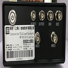
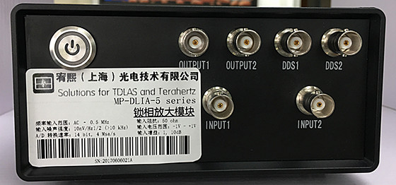
Dual-channel Lock-in Amplifier Module
Description
Phase-locked amplification and demodulation techniques of weak signals have a wide range of applications in Turnable Diode Laser Absorption Spectrum (TDLAS) gas sensoring, Atomic Force Microscope (AFM) and Electrostatic Force Microscope (EFM) field. In order to meet various customers requirements, Idealphotonics developed a dual-channel micro-DSP phase-locked amplifier which integrates modulated digital signal generation, digital detector signal collection, synchronous phase-locked demodulation all in one. The highly integrated amplifier is equipped with the signal processing function which is required in TDLAS, AFM,EFM and other applications. It provides a more cost-efficient solution for researching/ industrial labs, industrial products and other applications.
Features
Internal synchronized reference frequency, no external reference signal needed
Demodulate the weak signal down to 10nV with central frequency up to 400kHz
Two independent LIA channels (each with independent X/Y/R/demodulation)
Two DDS modulation outputs with respectively frequency, amplitude, and offset output signals adjustable
Two low speed analog channels, output the demodulation results in real time
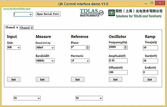
USB virtual serial port to connect the host PC, minimalist phase-locked control interface
Small size, portable, easy to integrate
Flexible to configure the FPGA algorithm according to customers requirements
Application
● TDLAS,
● AFM,
● EFM
PC Control Interface
PARAMETER
|
General |
|
|
Size |
10 cm x 11 cm |
|
Weight |
250 g |
|
Power Supply |
DC 5V/2A (within power supply board) |
|
Analog In |
|
|
Frequency |
AC – 0.5 MHz |
|
Input Impedance |
1 Mohm |
|
Input Noise |
10nV/Hz1/2 (>10 kHz) |
|
Voltage Range |
-1V - +1V |
|
Input Gain |
1, 10 |
|
A/D |
14 bit, 4 MSa/s |
|
Analog Output |
|
|
Output |
2 channels, -1V - +1V |
|
Frequency |
DC – 0.5 MHz |
|
D/A |
16 bit, 4 MSa/s |
|
Demodulator and the reference phase |
|
|
Number of channels |
2 channels (internal reference) |
|
Time constant |
1ms, 10ms (customized version available) |
|
Filter Bandwidth(Hz) |
|
|
Harmonic |
1F, 2F, 3F, 4F |
|
Reference phase resolution |
1.0 degree |
|
Auxiliary and others |
|
|
AUX Output |
2 channels, +-1V range |
|
D/A |
16 bit, 4 MSa/s |
|
D/A Analog Bandwidth |
10 kHz |
|
Standard PC Interface |
USB Virtual COM |
|
General PC I/O (GPIOs) |
UART, I2C, SPI |
|
PID Control |
(customized version available) |
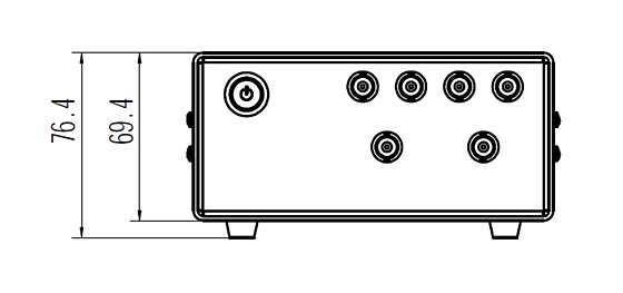
DIMENSIONAL OUTLINE

Application case
In this chapter tunable diode laser absorption spectroscopy (TDLAS) is briefly presented as an example for the application of lock-in amplifiers.

Fig. 3. Basic TDLAS principles of operation
TDLAS is an optical method for detecting trace concentrations of one or more selected gas species mixed with the other gases. A basic TDLAS setup consists of tunable diode laser light source, transmitting (i.e. beam collimation) optics,optically accessible absorbing medium, receiving optics (i.e. beam focusing),detectors and signal processing unit. The emission wavelength of the tunable diode laser (VCSEL, DFB, etc.) is tuned over the characteristic absorption lines of the species in the gas in the path of the laser beam. This causes a reduction of the measured signal intensity, which can be detected by a photodiode, and then processed in the signal processing electronics to provide an output indicating the gas concentration and other properties.To enhance the sensitivity in the TDLAS, laser wavelength modulation technique and phase-sensitive lock-in detection (wavelength modulation spectroscopy (WMS)) are employed. WMS involves the modulation of the laser wavelength via current at a high frequency. The interaovided by HealthyPhoton was designed to be used in TDLAS WMS applications, offering several advantages over direct absorption spectroscopy such as higher sensitivity, baseline free, calibration free, line-locking feasibility etc.
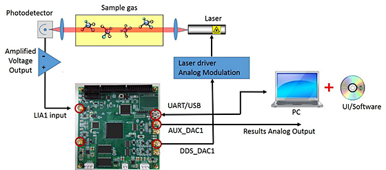
4. Cable connections for single channel TDLAS application
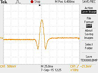
Fig. 5. A WMS 2f harmonic analog signal output acquired by an oscilloscope
Comparison test
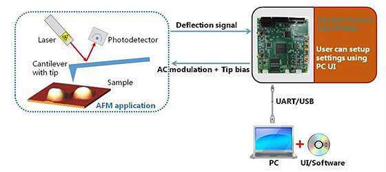
Detect surface micro-structure of SRAM chip sample by atomic force microscope (AFM).
AFM Experiment principle diagram
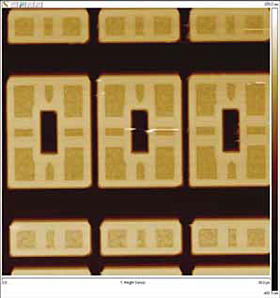
SRAM chip sample photo
 |
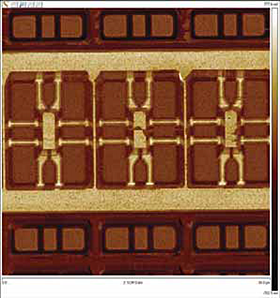 |
You can see the basic structure of SRAM chip as above. The left image shows the scanned surface structure of normal AFM around 30μm.The right image integrates with SCM (scanning capacitance microscopy) technologies, includes the surface struction of semiconductor adulterated information.
Samples are provided by Bruker Company.
Details:http://www.brukerafmprobes.com/Images/SCMSAMPLE%20App%20Note.pdf
The phase-locked amplifier used in the test:
Bottom left: AFM internal phase-locked amplifier image(IL)
Bottom Middle: One commercial phase-locked amplifier image(model SR7230)(SR)
Bottom Left: Idealphotonics phase-locked amplifier image
The time constants of all the phase-locked amplifiers used in this experiment are set as 1ms.
Image quality comparison
Under -5dB power, SCM output amplitude(dC/dV Amp) and Phase(dC/dV Phase)surface structure image quality comparison.
DV Amp

DC/dV Phase

Under -10dB power, SCM output amplitude(dC/dV Amp) and Phase(dC/dV Phase)surface structure image quality comparison.
DV Amp

DC/dV Phase

using the phase-locked amplifier developed by Idealphotonics independently can achieve clearer image and higher image SNR than AFM SCM.
Idealphotonics focus on providing low cost, high quality weak signal phase-locked amplifiers and other products for customers. Download software and Control SoftWare:
Maintenance and after-sales service:
After sales service:
Telephone:(852) 30786684 Email:info@idealphotonics.com
Packing List:
● 1 × IP-DLIA-5 series circuit board
● 1 × IP-DLIAPSB-5 power board
● 1 × USB flash drive containing configuration software and a PDF version of this guide
● 1 × mini-USB cable for connection to a Windows®PC
● 1 × 5VDC power cable


 编辑
编辑