|
info@idealphotonics.com
search
Home > 
Si High-Performance Avalanche Photodiode (APD) 400-1000nm 0.5mm TO-18
The QC30902EH high-performance silicon avalanche photodiode (APD) has a photosensitive surface diameter of 0.5 mm, making it suitable for biomedical and analytical applications. This SiAPD is designed with a dual-diffusion "penetrating" structure that offers high responsiveness between 400 nm and 1000 nm, as well as extremely fast rise and fall times across all wavelengths. The device's responsiveness is independent of modulation frequencies up to approximately 800 MHz. The detector chip is sealed behind a flat glass window in a modified TO-18 package. Models include C30902EH/C30902EH-2, C30902SH, and C30902SH-TC.
Product features:High quantum efficiency: 77% at 830 nm 、The C30902SH and C30921SH can operate in Geiger mode 、C30902EH/SH-2 type, with built-in 905 nm filter 、C30902BH type, with spherical lens 、Sealed packaging 、Low noise at room temperature 、High responsivity – internal avalanche gain over 150 、Spectral response range – 400 to 1000 nm (at the 10% Q.E. point) 、Time response – typically 0.5 ns 、Wide operating temperature range – from -40°C to +70°C 、RoHS compliant
Application area:Lidar 、 Distance measurement 、Low-signal fluorescence 、Photon counting 、Barcode scanning
Unit Price
Please contact customer service for a discounted quote.
Part Number
C30902EH
Lead Time
Please contact customer service for lead time.
Stock
Please contact customer service for stock availability.
Add to Inquiry
Inquire online
General Parameters
Dimensional Drawing

C30902 and C30921 Series
High-speed solid-state detectors for low-light applications

The C30902EH series avalanche photodiodes are highly suitable for a wide range of applications, including lidar, ranging, small signal fluorescence, photon counting, and barcode scanning. The C30902EH series avalanche photodiodes from Excelitas Technologies are manufactured with a dual-diffusion "penetrating" structure. This design provides high responsiveness between 400 nm and 1000 nm, along with extremely fast rise and fall times across all wavelengths. The device's responsiveness is independent of modulation frequencies up to 800 MHz. The detector chip is sealed behind a flat glass window in an improved TO-18 package. The effective diameter of the photosensitive surface is 0.5 mm.

The C30921EH is packaged in a TO-18 light pipe, allowing effective coupling of light from a focal point or fiber optic with a diameter of up to 0.25 mm to the detector. The sealed TO-18 package allows for fiber optic matching with the light pipe end to minimize signal loss without compromising the stability of the detector. The C30902EH-2 or C30902SH-2 (sealed TO-18 package with a built-in 905 nm band-pass filter) and C30902BH (sealed ball lens) form part of the C30902 series.

The C30902SH and C30921SH models feature photodiodes with extremely low noise and dark current. They are suitable for ultra-low light-level applications (optical power less than 1 pW) and can be used as photon counters in normal linear mode (VrVbr) with gains of up to 250 or higher, where a single photoelectron can trigger an avalanche pulse with approximately 10^8 carriers. In this mode, no amplifier is needed, and the single-photon detection probability can be as high as approximately 50%.

Photon counting is also advantageous in gated and compliant technologies used for signal retrieval.


Electro-optical characteristics

Test conditions: Housing temperature = 22°C, unless otherwise specified, please refer to the notes on the following page.


C30902EH/C30902EH-2

C30902SH

C30902SH-TC


Detector Type

C30902BH

C30902SH-2

C30902SH-DTC


C30921EH

C30921SH

Parameter

Min

Typ

Max

Min

Typ

Max

Min

Typ

Max

Units

Photosensitive zone


Effective diameter

0.5

0.5

0.5

mm

Active area

0.2

0.2

0.2

mm2

Phototube characteristics (C30921)


Numerical aperture of the phototube

0.55

0.55

[no units]

Core refractive index (n)

1.61

1.61

[no units]

Core diameter

0.25

0.25

mm

Field of view α


With standard/spherical lens window
Built-in 905 nm filter -2

90
55

90
55

122
N/A

Degrees

With light tube (in air)

33

33

N/A


Field of view α’


With standard window

114

114

129

Degrees

spherical lens (-2) built-in 905 nm filter

78

78

N/A


Breakdown voltage, Vbr


225


225


225


V

Reverse bias temperature coefficient, Vr, constant gain voltage

0.5

0.7

0.9

0.5

0.7

0.9

0.5

0.7

0.9

V/。C

Detector temperature


-TC

0

C

-DTC

-20

C

Gain


150


250


250


Responsivity


At 830 nm (not applicable to -2)

70

77

117

128

128

A/W

at 900nm

55

65

92

108

108

A/W

Quantum efficiency


at 830 nm

77

77

77

%

at 900 nm

60

60

60

%

Dark current, id


15

30


15

30


15

30

nA

-TC (at 0。C)


2


nA

-DTC (at -20。C)


1


nA

Noise current, in (see note 3)
-TC (at 0 °C)


0.23

0.5


0.11

0.2


0.04


pA/ÖHz

-DTC (at -20。C)


0.02

pA/ÖHz

capacitance


1.6

2


1.6

2


1.6

2

pF

Rise/Fall time, RL=50 Ω
10% to 90% points


0.5

0.75


0.5

0.75


0.5

0.75

ns

90% to 10% points

0.5

0.75

0.5

0.75

0.5

0.75

ns

Maximum driving current


-TC

1.8

A

-DTC

1.4

A

Maximum bias voltage


-TC

0.8

V

-DTC

2

V

Dark count rate at 5% photon detection (at 830 nm)
probability (830 nm)


5000

15000


1100(-TC)
250(-DTC)

15000

cps

When the voltage exceeds Vbr, the photon detection probability is 5% (at 830 nm)


2


2


V

Pulse ratio probability after 5% photon detection (at 830 nm)


2

15


2


%

Under specific DC reverse operating voltage, Vop or Vr, as provided for each device, the spot diameter is 0.25mm (C30902EH, SH) or 0.10 mm (C30921EH, SH). When operating at voltages between 180V and 250V, the device will meet the above electrical characteristic limits.

The temperature of the thermistor (in Kelvin) can be calculated using the following formula:
[K]=β⋅(RR∞)[K] = β \cdot \left(\frac{R}{R∞}\right)[K]=β⋅(R∞R)
where R is the measured resistance of the thermistor in ohms, β = 3200, R0 = 5100Ω, T0 = 298.15 K, and r∞ = -βRe ≈ 0.1113.

Table 2 – Maximum Rated Values

The theoretical expression for the shot noise current in an avalanche photodiode is:
in=(2q(Ids+(IdbM2+PORM)F)BW)1/2i_n = \left( 2q \left( I_{ds} + ( I_{dbM2} + P_{ORM} ) F \right) BW \right)^{1/2}in=(2q(Ids+(IdbM2+PORM)F)BW)1/2
where q is the electronic charge, IdsI_{ds}Ids is the dark surface current, IdbI_{db}Idb is the dark body current, F is the excess noise factor, M is the gain, P_O is the optical power on the device, and BW is the noise bandwidth. For these devices, F=0.98(2−1M)+0.02MF = 0.98 \left( 2 - \frac{1}{M} \right) + 0.02MF=0.98(2−M1)+0.02M (Reference: PP Webb, RJ McIntyre, JJ Conradi, "RCA Review").

C30902SH and C309021SH can operate at higher detection probabilities (see Geiger mode operation section).

Pulses occurring 1μs to 60 seconds after the main pulse.

Parameter

Symbol

Min

Max

Units

Storage Temperature

TS

-60

100

°C

Operating Temperature

Top

-40

70

°C

Soldering for 5 seconds (leads only)


260

°C

Room Temperature Reverse Current


Average value, continuous operation

200

μA

Peak value (1s duration, non-repetitive)

1

mA

Room Temperature Forward Current


Average value, continuous operation

IF


5

50

mA

mA

Peak value (1s duration, non-repetitive)


60

mW


Electro-optic Characteristics

1.png

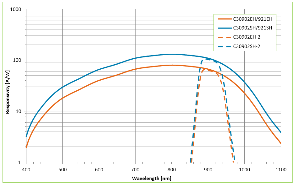
Figure 1 – Typical Spectral Responsivity at 22°C Shell Temperature


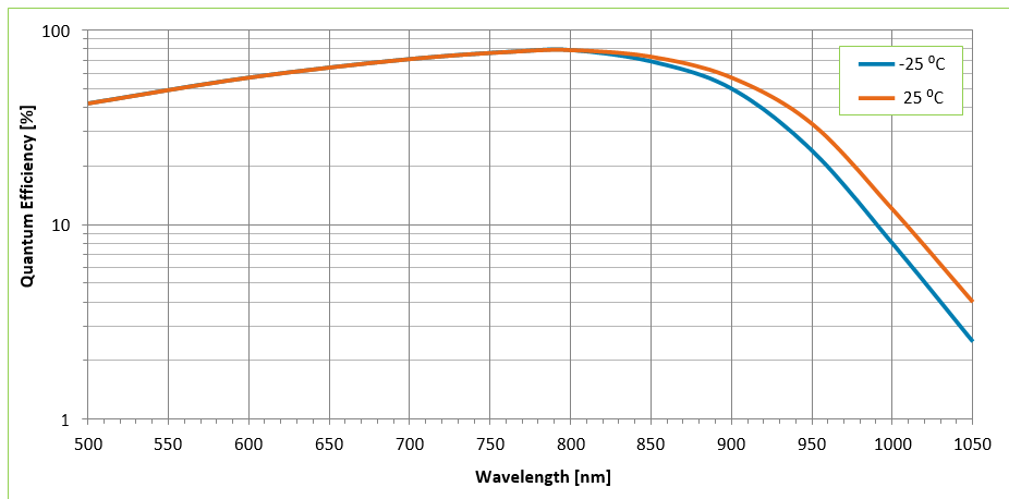
Figure 2 – Typical Quantum Efficiency vs Wavelength Relationship as a Function of Shell Temperature


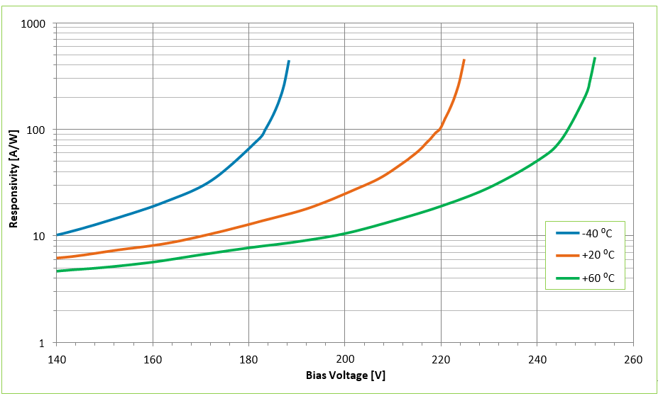
Figure 3 – Typical Responsivity vs. Operating Voltage at 830 nm (as a Function of Shell Temperature)


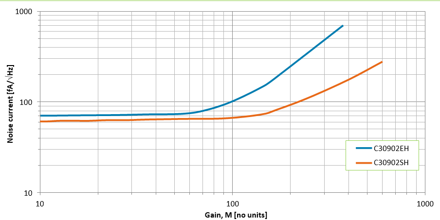
Figure 4 – Typical Noise Current vs. Gain


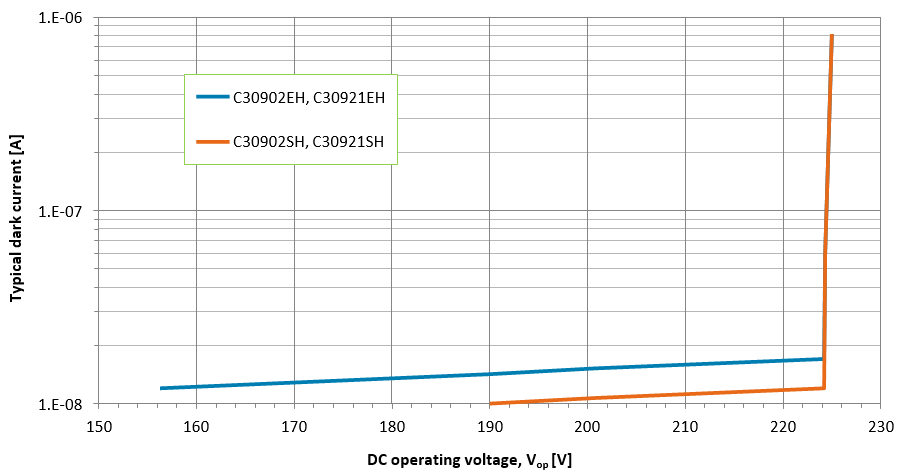
Figure 5 – Typical Dark Current vs. Operating Voltage at a Shell Temperature of 22°C


6.png

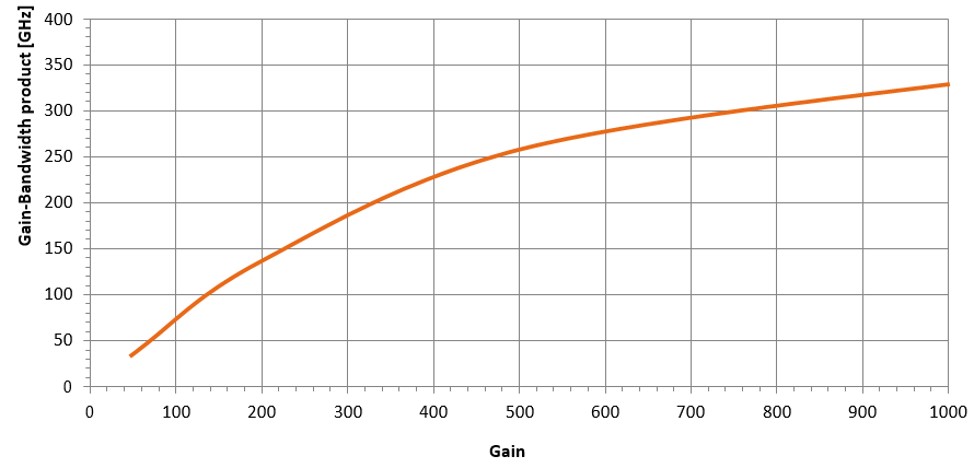
Figure 6 – Typical Gain – Bandwidth Product as a Function of Gain at a Shell Temperature of 22°C


7.png

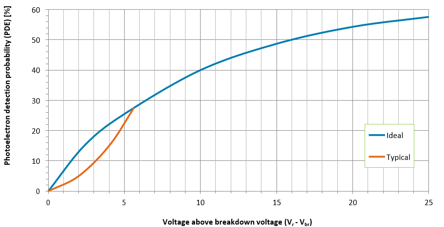
Figure 7 – Geiger Mode, Photon Detection Probability at 830nm as a Function of Voltage Above Vbr at a Shell Temperature of 22°C


8.png

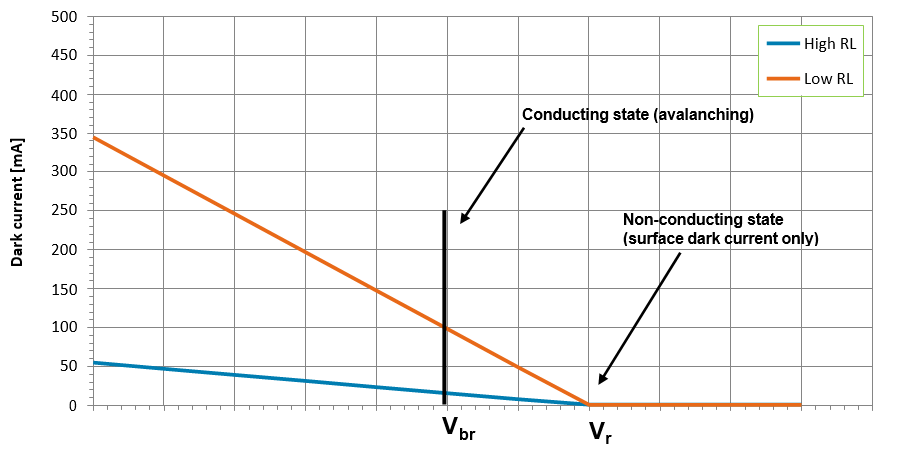
Figure 8 – Load Line of C30921SH in Geiger Mode


9.png

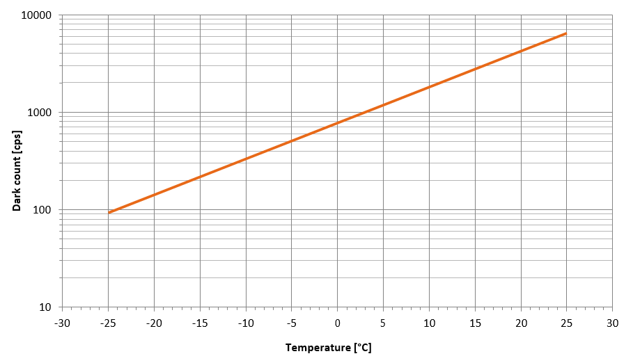
Figure 9 – Typical Dark Counts vs. Temperature at 5% Photon Detection Efficiency (830nm)


10.png

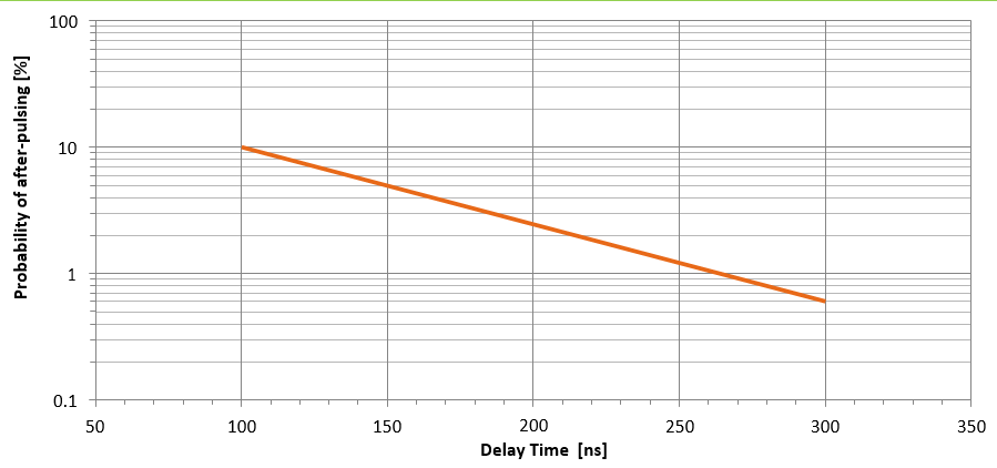
Figure 10 – Probability of the Next Afterpulse within 100ns vs. Delay Time in Active Quenching Circuit (Typical for C30902SH and C30921SH at Vbr, Shell Temperature at 22°C)


Packaging Drawing (Other packaging can be provided upon request)

11.png

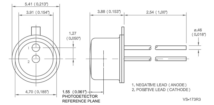
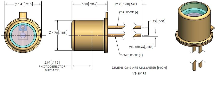
Figure 11 – Reference Dimensions for C30902EH and C30902SH, in Millimeters (Inches)


12.png

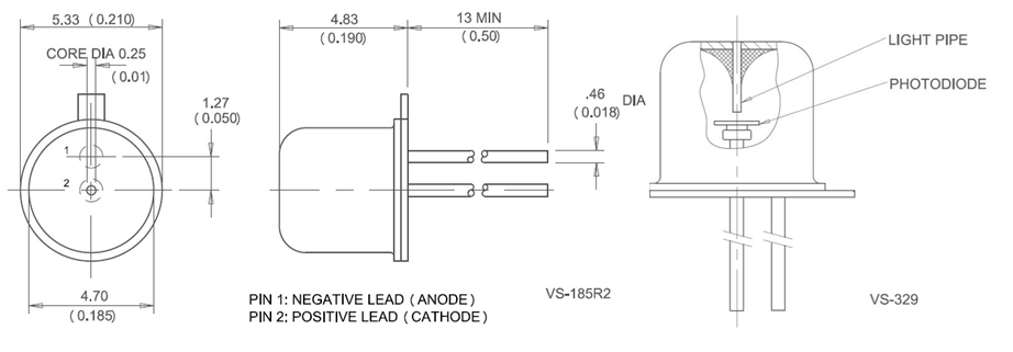
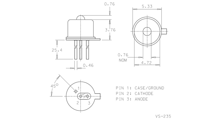
Figure 12 – Packaging Outline and Section of the Lamp Tube for C30921EH and C30921EH, Reference Dimensions Displayed in Millimeters [Inches]


13.png

Figure 13 – Reference Dimensions for C30902EH-2 and C30902SH-2, Displayed in Millimeters [Inches]


14.png

Figure 14 – C30902BH, Reference Dimensions in Millimeters


15.png

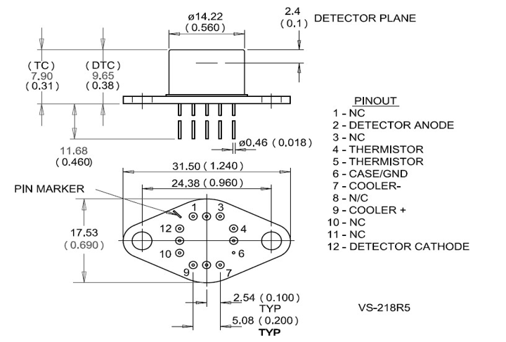
Figure 15 – C30902SH-TC/-DTC, TO-66, Flanged Profile, Reference Dimensions in Millimeters (Inches)


16.png

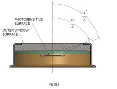
Figure 16 – Approximate Field of View – C30902 and C30921 Series

Angle of incident radiation ≤ a/2, the photosensitive surface fully illuminates.

Angle of incident radiation > a/2 but ≤ a/2, the photosensitive surface partially illuminates.


 “-TC” and “-DTC” TE Cooling Versions TE-cooled APDs are used for various reasons (Figure 15). Most applications benefit from the -TC (single) or -DTC (dual) versions for two reasons:

As mentioned earlier, they reduce thermal noise used for very small signal detection. The TC version is designed to operate the APD down to 0°C, while the DTC version can operate at -20°C when the ambient temperature is 22°C.

Maintain a constant APD temperature regardless of ambient temperature. Since the APD breakdown voltage decreases as the temperature decreases, the TE cooler allows a single operating voltage. Moreover, this configuration enables the APD to maintain consistent performance over an extended temperature range. The thermistor inside the device can monitor the APD temperature and can be used to implement a TE cooler feedback loop to maintain a constant APD temperature and/or to provide temperature compensation for the APD bias voltage. A suitable heat sink is needed to dissipate the heat generated by the APD and TE cooler.

Custom Design Recognizing that different applications have different performance requirements, Excelitas offers a broad range of customizations for these APDs to meet your design challenges. Dark count selection, custom device testing, and packaging are just some of the application-specific solutions.

Geiger Mode Operation When the bias voltage exceeds the breakdown voltage, the avalanche photodiode typically conducts large currents. However, if the current is limited to less than a specific value (about 50 for these diodes), the current becomes unstable and can turn off by itself. The explanation for this phenomenon is that the number of carriers in the avalanche region at any time is small and fluctuates greatly. If the number fluctuates to zero, the current must stop. If it remains off, it will stay in that state until the avalanche pulse is triggered again by a large block or photogenerated carriers.

Select the "S" type to produce small dark current in batches. This makes them suitable for low-noise operation below VBR in Geiger mode or photon counting above VBR. In this so-called Geiger mode, a single photoelectron (or thermally generated electron) can trigger an avalanche pulse, causing the photodiode to discharge from its reverse operating voltage Vr to a voltage slightly lower than VBR. The probability of this avalanche occurring, as shown in Figure 7, is referred to as the "photoelectron detection probability." It increases as the reverse voltage Vr increases. For a given Vr and Vbr value, the photoelectron detection probability is independent of temperature. To determine the photon detection probability, the photoelectron detection probability should be multiplied by the quantum efficiency, as shown in Figure 2. Quantum efficiency is also relatively independent of temperature, except near the 1000 nm cutoff.

The "S" type can be used in Geiger mode with either a "passive" or "active" pulse quenching circuit. Below, the advantages and disadvantages of each method are discussed.

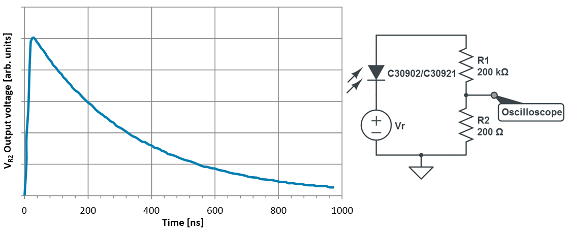
Passive Quenching Circuit The simplest and, in many cases, a perfectly suitable method to quench breakdown pulses is by using a current-limiting load resistor. This "passive" quenching is illustrated in Figure 17. The circuit’s load line is shown in Figure 8. To be in the conducting state at Vbr, two conditions must be met:

The avalanche must be triggered by photoelectrons or electrons generated within the diode’s avalanche region (Note: Holes in silicon have a very low efficiency in triggering the avalanche).

In order to remain in the conducting state, there must be enough current (called the latch current ILATCH) flowing through the device to maintain the presence of electrons or holes in the avalanche region. Typically, for C30902SH and C30921SH, ILATCH = 50uA. For currents far greater than ILATCH (Vr > Vbr) / RL, the diode stays conducting. If the current (Vr > Vbr) / RL is much less than ILATCH, the diode will almost immediately switch to a non-conducting state. If (Vr > Vbr) / RL is approximately equal to ILATCH, the diode will randomly switch between the conducting and non-conducting states depending on the statistical fluctuations in the number of electrons and holes in the avalanche region reaching zero.

When RL is large, the photodiode conducts normally, and in the non-conducting state, the operating point is at Vr - IDSRL. After avalanche breakdown, the device is recharged to voltage Vr - IDSRL with a time constant of RLC, where C is the total capacitance of the device, including stray capacitance. Using C = 1.6 pF and RL = 200 kΩ, the calculated recharge time constant is 0.32 μs. The rise time is fast, ranging from 5 to 50 ns, decreasing as Vr - Vbr increases, and is highly dependent on the load resistor, leads, and capacitor capacitance.

 17.png 

Figure 17 – Example of a passive quenching circuit


Active Quenching Circuit
Before the C30902SH is charged, the probability of detecting another incident photon is relatively low. To avoid excessive dead time when operating at high voltages above Vbr, an "active quenching" circuit can be used. After detecting an avalanche discharge, the circuit temporarily reduces the bias voltage for a fraction of a microsecond. This delay time allows all electrons and holes to be collected, including those that are temporarily "trapped" in different impurity sites within the silicon. When a higher voltage is re-applied, there are no electrons in the depletion region to trigger another avalanche or lock the diode. The charging can be very rapid through a small load resistor. Alternatively, the bias voltage can be maintained, but the load resistor can be replaced by a transistor that remains off for a short period after the avalanche, then turns on for enough time to charge the photodiode.

Timing Resolution
For photon counting applications, the timing resolution or time jitter is the time it takes for a TTL trigger pulse to be detected after a photon is detected, plotted and averaged at the half-height of the curve. The jitter at the half-voltage point is typically on the order of the rise time. For timing applications that require minimal jitter, the lowest possible threshold for the rise pulse should be used.

Post-Pulse
A post-pulse follows the photon-generated pulse and is induced by its avalanche breakdown. The post-pulse is typically caused by one of approximately 10^8 carriers that pass through the diode during the avalanche. As mentioned earlier, this electron or hole is captured and trapped at an impurity site within the silicon. When this charge carrier is released, typically within less than 100 nanoseconds but sometimes a few milliseconds, it may trigger another avalanche. Using the circuit shown in Figure 17, the probability of a post-pulse occurring more than 1 microsecond after a voltage above Vbr + 2V is usually less than 1%.

The post-pulse increases with the bias voltage. If the post-pulse needs to be reduced, it is recommended to keep Vr - Vbr at a low level, use an active quenching circuit with a long delay line, or use a passive quenching circuit with a long RLC constant. The stray capacitance must also be minimized. In some cases, electronic gating of the signal may be applied. If the post-pulse is a significant complication in a specific application, it may be worth considering operating below Vbr with a good amplifier.

Dark Current
The "S" version has been selected for its lower dark count rate. Cooling to -25°C reduces the dark count rate by approximately 50 times due to its exponential dependence on temperature.

The dark count increases with the voltage, and its curve mirrors the photon detection probability until the voltage triggers a feedback mechanism after the pulse, significantly increasing the dark count rate. This maximum voltage depends on the circuit and is not guaranteed beyond the values listed in Table 1. In most cases, with a delay time of 300 nanoseconds, the diode can effectively operate at voltages up to Vbr + 25V.

The C30902 should not be forward biased, nor should it be exposed to strong illumination in the absence of bias. These conditions significantly enhance dark counts, and it may take 24 hours for the device to return to its nominal value.

RoHS Compliance
The design and manufacturing of the C30902 and C30921 series avalanche photodiodes are fully compliant with the EU Directive 2011/65/EU - Restriction of the use of certain hazardous substances in electrical and electronic equipment (RoHS).

Warranty
A standard 12-month warranty applies after shipment. Any warranty is void if the photodiode window has been opened.

About Excelitas Technologies
Excelitas Technologies is a global technology leader committed to providing innovative, customized solutions to meet the lighting, detection, and other high-performance technology needs of OEM customers.

From PerkinElmer, EG&G, and RCA, Excelitas has been serving our OEM customer base with photodetectors and modules for over 45 years. We remain committed to innovation and providing the highest quality solutions to our global customers.

From aerospace and defense to analytical instruments, clinical diagnostics, medical, industrial, and security applications, Excelitas Technologies is dedicated to helping our customers succeed in their professional markets. Excelitas Technologies employs approximately 3,000 people in North America, Europe, and Asia, serving customers worldwide.

Product Recommendation